11 kv capacitor bank (tepco) Capacitor bank diagram step multiple banks fuses Step-by-step tutorial for building capacitor bank and reactive power
Discharge behavior of capacitor banks
Capacitor shunt
Step-by-step tutorial for building capacitor bank and reactive power
Protection of capacitor banks by fuses during energization andSwitchable capacitor bank or switched capacitor bank Capacitor ocl 25v amplifier connection wiring schematicStep-by-step tutorial for building capacitor bank and reactive power.
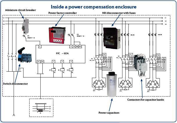
Power factor correction capacitors sizing calculations – part eighteenPower compensation factor reactive correction capacitors capacitor bank sizing used inside panels cables size eighteen calculations part pfc ☑ components of a capacitor bankBank capacitor diagram wiring electrical phase circuit power building compensation step reactive control panel portal engineering tutorial.
Capacitor banks overvoltage inmr
Capacitor bank diagram wiring power ac step panel reactive circuit building wire switchgear tutorial supplying main connectCapacitor switchable switched electrical4u Capacitor bank diagram banks schematic characteristics applications figureCircuit main bank capacitor panel power connection reactive step cb breaker compensation l1 represents reactors l2 dots capacitors l3 bars.
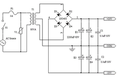
Capacitor bank schematic capacitors discharge voltage high parallel banks pulse assume network let25v capacitor bank for ocl amplifier circuit diagram Overvoltage protection of series capacitor banksDischarge behavior of capacitor banks.

3 phase capacitor bank wiring diagram
Capacitor banksPower factor correction capacitor wiring diagram Capacitor correction banksCapacitor kv tepco schematic.
.